
At Hot Chips 2026, SK Hynix laid out its advanced packaging roadmap for HBM (High Bandwidth Memory), introducing Intel EMIB as a 2.5D option and setting a long‑term goal of 3D‑stacked HBM‑on‑accelerator integration.
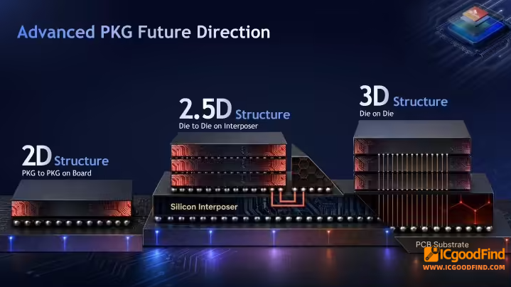
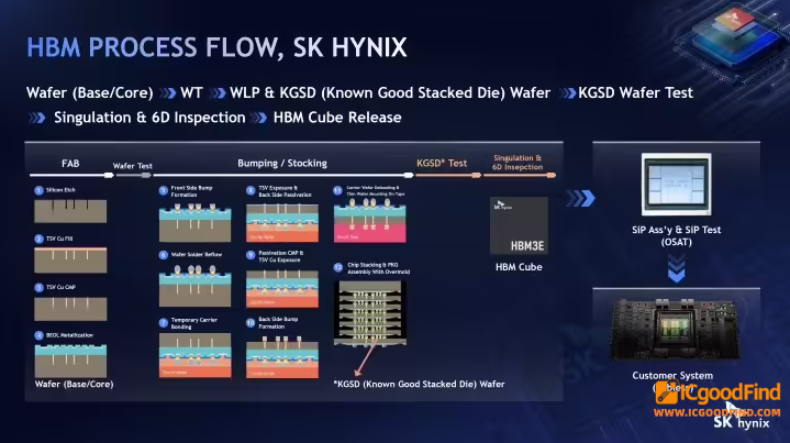
Current HBM: uses TSV to stack up to 16 DRAM dies on a base die, then connects via 2.5D packaging over a silicon interposer. A 4‑stack HBM3E delivers 144GB capacity, 4TB/s bandwidth at half the footprint of GDDR6.
HBM4 (now in production):
24Gb per die, up to 36GB per stack (48GB max), 2048‑bit interface, 8Gbps/pin → 2TB/s bandwidth
Power efficiency +40% vs. HBM3E, thermal performance +14%
12‑Hi in production; 16‑Hi in certification (775µm height, 16k+ microbumps, 20k+ TSVs)
Packaging battle: SK Hynix uses MR‑MUF for 16‑Hi HBM3E (with warp‑control and fine‑gap fill enhancements). But as bandwidth doubles every two generations, thermal load rises 2.2x – pushing the company to adopt hybrid bonding as the next core technology. Hybrid bonding allows 24% thicker dies, <18µm TSV pitch, 35% lower thermal resistance, and the potential to break the 16‑layer stack limit.
For thermal management, SK Hynix introduced I‑HBM – embedding high‑conductivity insulative heat spreaders over hot spots, cutting thermal resistance by >30%. Longer‑term, the company plans to double TSV count, leverage advanced logic processes for higher IO speeds, and use power‑TSVs to optimize PDN.
On 2.5D interposers, SK Hynix now evaluates Intel EMIB alongside Nvidia’s CoWoS‑L/R/S options – sparking renewed market talk of an Intel‑SK Hynix memory JV. The ultimate goal: 3D stacking HBM directly onto the accelerator die once logic and packaging technologies mature.
ICgoodFind Takeaway:
SK Hynix is diversifying HBM packaging – hybrid bonding, EMIB, and I‑HBM all point to fiercer tech competition in AI memory. The race to lower thermal and boost bandwidth is far from over.
